


2D & TMD Materials
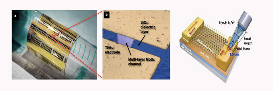
Flexible MoS2 TFTs
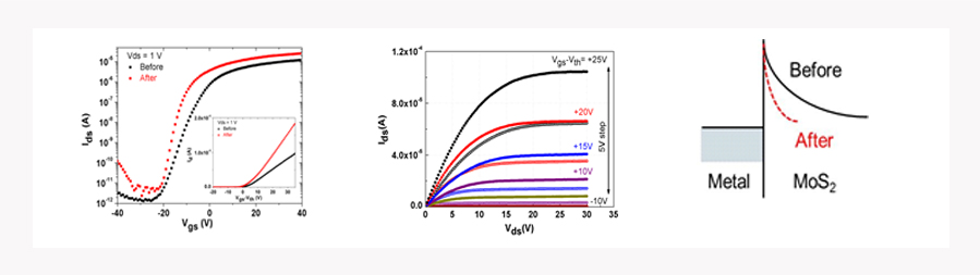
 Electrical properties
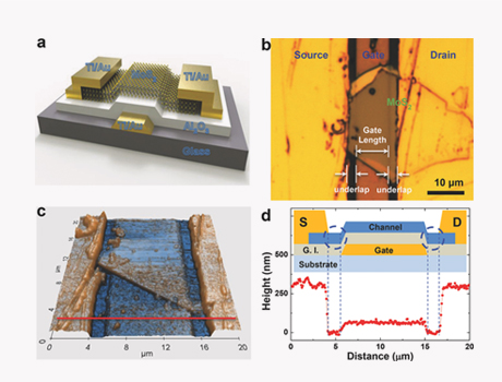
 Local-gate multilayer MoS2 phototransistor
- Channel: mechanically exfoliated MoS2 flakes
- Gate dielectrics: Al2O3/SiO2
- Metal contacts: Ti/Au
- Substrates: flexible PEN
- Contact annealing: Nd:YVO4 pico-second pulsed laser
Electrical properties
- Transfer characteristics : on-current and field-effect mobility increase
- Output characteristics: output resistance increases
- Suggested mechanism: laser annealing on contacts → increased carrier concentration at the junction → reduced tunneling
barrier width
Local-gate multilayer MoS2 phototransistor
Multilayer MoS2 phototransistor in a local bottom-gate structure. a) 3D schematic figure of a local bottom-gate MoS2 phototransistor. b) Optical microscopy image and c) 3D AFM topographic image of the device, showing ungated MoS2 channel regions (gate underlap) between the gate and the source/drain electrodes. d) Topological analysis of line profile data obtained along red line in Figure c. (Inset) Cross-sectional view of the device.
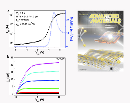
a) Transfer characteristic (Ids−Vgs) curve and field-effect mobility of the local bottom-gate multilayer MoS2 phototransistor at Vgs= 1 V. b) Output characteristic (Ids−Vgs) curves of the same device with different gate biases (Vgs−Vth = 4, 5, 6, 7, 8, and 9 V).